Stereo Vision ASIC

home / Deutsch

semester thesis project (winter 02/03)

As part of the lectures on VLSI chip design at the Integrated Systems Laboratory of the Swiss Federal Institute of Technology (ETH) students get the opportunity to design their own ASIC. The whole design cycle from algorithm design to silicon testing can be experienced. Together with Michael Kuhn and Oliver Isler, we developed  a real-time stereo vision chip. An extensive algorithm design and evaluation (Java) was followed by three months of VHDL coding and simulation as well as the backend design. In early 2003, the chip was fabricated on a UMC 250nm process. The chips were finally tested on HP test equipment of the institute and worked. The design was published at MWSCAS 2003 in Cairo. See the paper (pdf, 142k) for further information or browse the complete project documentation (pdf, 742k).

Stereo Vision

The idea of stereo vision is to calculate spatial depth from two horizontally displaced camera images. Since the two cameras show two different viewpoints of the same scene, perspective shifts ('displacements') of objects can be determined. From the displacement of an object, an estimate of its spatial position can be calculated. If this estimate is calculated for each point within the scene, a depth map forms. Within the depth map, color represents spacial depth.

stereo vision principle (two camera images and a depth map)
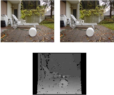
Top images: two horizontally displaced camera images of a scene
Bottom image: The corresponding depth map with light colors for near regions and dark colors for distant objects

Since calculating depth maps is a computationally intensive task, the idea of an ASIC doing the job real-time came up. In this way, stereo vision could be used for dynamic scenes like street traffic, collision avoidance or mobile robot navigation.

The Chip

The ASIC works on images of size 256*192 with 256 gray scales. Running with 75MHz it achieves more than 50 frames per second (fps), which corresponds to roughly 18 GOps. It occupies an area of only 2.56mm^2 on an UMC 0.25um 5metal process.

photo of bonded chip microscopic silicon image
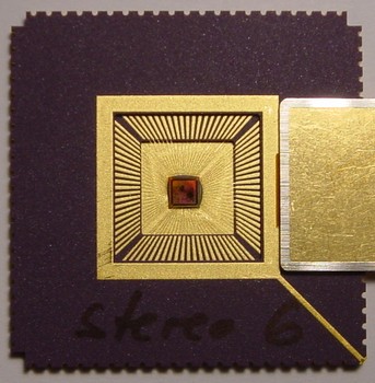
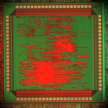
Left: image of opened chip package. Right: Microscopic view of the silicon


last update: 22.2.04 Stephan Moser